Our experts on FPD China and Plansee products

FPD China 2024 took place in Shanghai, China from 20-22 March 2024. Plansee once again exhibited at the international trade fair, organised by SEMI and others, with a new and modernised stand design. At our stand, our team showcased to customers a range of molybdenum, tungsten, tantalum, niobium and chromium components that are overcoming the challenges of conventional materials when used in advanced flat panel displays, energy-efficient LED products and environmentally friendly fuel cells.
Many customers visited our stand and interesting discussions took place. We would like to thank all customers who visited our booth at FPD and we are looking forward to FPD China 2025.
Our experts on FPD China and Plansee products


Exhibits at the FPD China

Customer meetings at the Plansee stand

Customer meetings at the Plansee stand

hot zone model

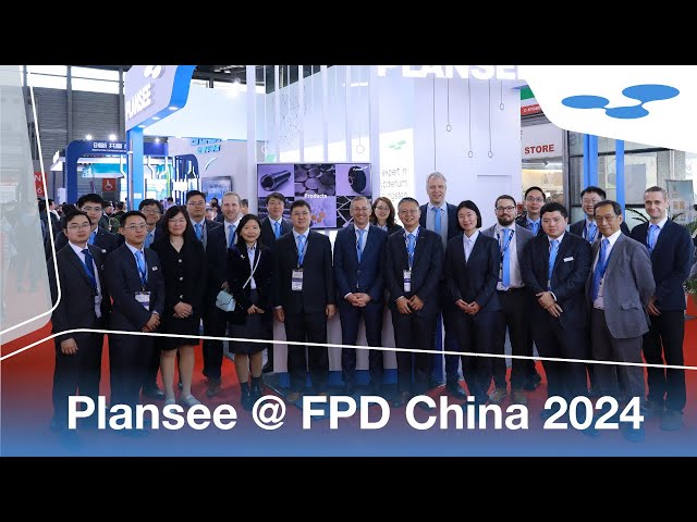
The entire Plansee team in front of the newly designed stand
Plansee specializes in the manufacture of molybdenum and tungsten products for the electronics industry and our display production products meet all the essential requirements. The highest quality, best material purity, and the highest density ensure high-quality results for modern displays, ensuring every pixel on every display shines in its full brilliance.
From producing the glass and semiconductors right through to coating the displays, we know exactly what you need. As a reliable and sustainable partner, we work very closely with our customers to tailor the material properties and tolerances of our products precisely to their requirements. We are making continual investments in the latest fully automatic systems to guarantee high production capacities, reproducible process quality, and a reliable delivery capability. We also offer global refurbishment services to increase the share of reusable products on the market. What's more, we supply components for crystal growth, which are used in the LED and photovoltaics industries. Different molybdenum and tungsten components are used in high-temperature furnaces or crystal growth systems to draw sapphire or silicon ingots.
The online catalogue with 3D exploded views and OEM references for over 30 plant types
Ion implantation online catalogueFDP China—the international industrial exhibition for displays and touchscreens—brings together equipment, materials, and the latest technologies in the production chain. Since 2004, FDP China has maintained strategic partnerships with a range of organizations in the FPD industry, both in China and abroad.