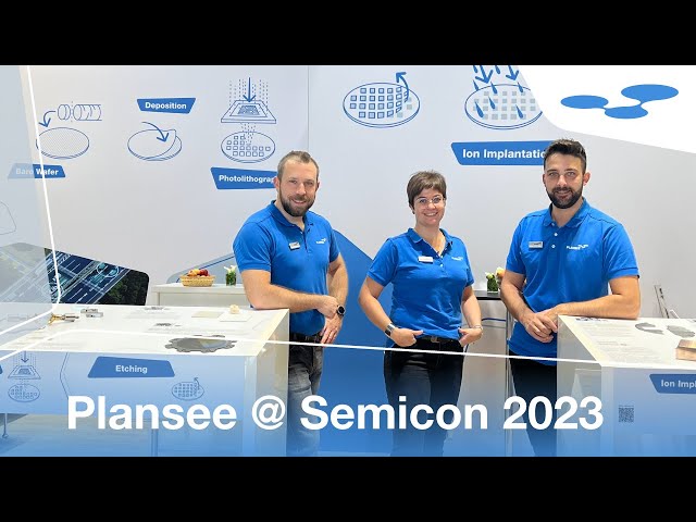
Our Plansee Team about the Semicon, products and applications

From November 14 to 17, Plansee had its own booth at SEMICON Europa in Munich for the first time. Several product groups were combined for the trade fair appearance in order to present our Wafer Journey to visitors: from the production and processing of the bare wafers to deposition, photolithography, etching, ion implantation and chip assembly (packaging) in the end.
We would like to thank all visitors and customers who visited us at our booth at Semicon 2023.
Our Plansee Team about the Semicon, products and applications

Plansee Booth

Team at our booth

Plansee Booth

Plansee give aways

Semiconductor base plates in detail

Our experts on site


We are a leading provider of products and solutions for the entire semiconductor supply chain and the world's largest manufacturer of powder-metallurgical components made from high-performance materials. Our primary focus lies in lithography, etching, thermal evaporation, PVD coating, ion-beam treatments, ion implantations, MOCVD, and IC packaging. We also offer global refurbishment services to increase the share of reusable products on the market.
After over a century working with molybdenum, tungsten, tantalum, and their alloys, we have all the necessary expertise to realize even the most demanding projects: from the development of new products and components through to the design and machining of complex parts. With decades of experience in the industry, we know the market inside out and exactly what our customers need.
Plansee is present in 28 countries around the world, including 12 production plants in Europe, Asia, and the USA. We are therefore in a position to ensure a reliable global supply chain for your products, components, and assemblies.
The online catalogue with 3D exploded views and OEM references for over 30 plant types
Ion implantation online catalogueOur videos give you an insight into the PVD sputtering process, the use of high-performance materials and clean room assembly at Plansee:

The PVD sputtering process
Molybdenum and tungsten in the thin-film industry
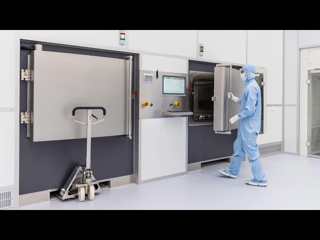
Clean room assembly at Plansee

SEMICON Europa 2023 takes place alongside productronica in Munich and is the largest trade fair for microelectronics in Europe. The trade fair is geared towards all decision-makers across the microelectronics supply chain.