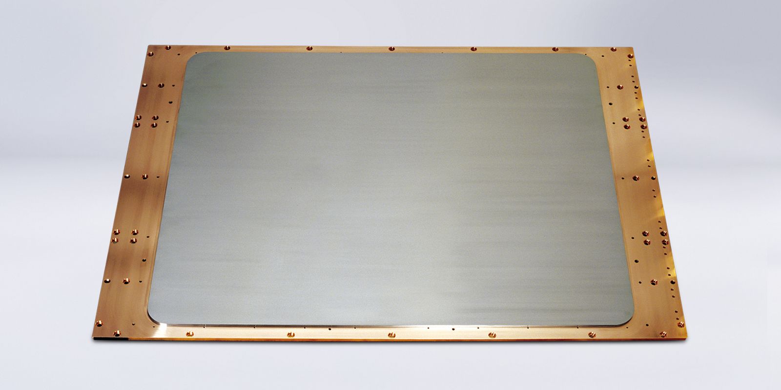
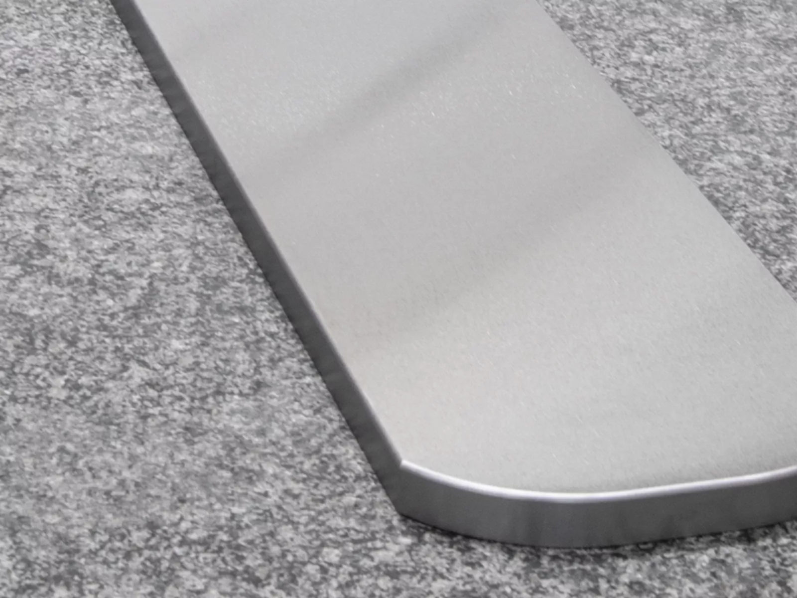
During the magnetron sputtering process (PVD process), tiny metal particles are released from sputtering targets, which settle as a thin film on a material to be coated (substrate). This process is a cost-effective and fast coating process in which all materials must satisfy the most stringent quality criteria.

Molybdenum sputtering targets
Molybdenum layers are the main components of thin-film transistors in TFT-LCD and OLED screens. They control the individual pixels at lightning speed, thereby guaranteeing particularly sharp images. Molybdenum layers are also used for other purposes. For example as the back contact in thin-film solar cells (CIGS, CdTe) and in microelectronics components (frequency filters, lithography).
Your advantages at a glance:
High purity
> 99.97%Maximum density
> 99.5%Homogeneous microstructure
Center of expertise for new coating solutions
Download our product specifications:
How are molybdenum layers produced?

Maximum purity
Our targets fulfill stringent purity requirements. The main advantages: excellent electrical conductivity of the layer and minimum particle formation during the PVD process. Metal and non-metal impurities in the sputtering target are transferred to the sputtered functional layer, thereby affecting its function or causing particle formation in the PVD process (arcing effect).
We guarantee that our molybdenum targets have a minimum purity of 99.97%. The typical purity of our molybdenum targets is 99.99%. This is how we guarantee that the layers produced satisfy the stringent requirements.
Maximum density and homogeneous microstructure
Our molybdenum sputtering targets are highly consolidated by means of special forming processes. This results in increased coating rates and improved coating properties in the PVD coating process. The advantages of this lie in the efficiency of the thin film production as well as a high output.
We can adjust the microstructure of the coating material in a targeted manner by means of our manufacturing process. With an evenly formed microstructure of the sputtering targets, you can achieve consistent sputtering rates and film thicknesses.
Center of expertise for new coating solutions
In the PVD coating process, everything must be perfectly matched. It is only if all process parameters are perfectly matched that the layer that suits the customer's exact requirements can be produced. We carry out sputtering under practical conditions in our PVD application laboratory. Our developer team creates layers here and analyzes them in detail according to defined specifications. This means that new coating materials are developed in a very short time in cooperation with customers and numerous development partners. Having worked with system manufacturers and OEMs for several years, we are directly involved in the latest developments and optimizations
Wide selection of target formats

We produce planar and tubular molybdenum targets in a single- and multi-part design for all common dimensions and coating systems.
Single-part planar targets can be series produced up to a size of 1.8 x 2.3 m. Multi-part planar target sets can be flexibly produced with a maximum length of the individual parts of up to 3.5 m.
We produce rotary targets in lengths of up to 4 m in a single- or multi-part design. Further information can be found on the product page:
Take a look at a few example applications for our coatings here:

Highest quality from a single source
We have the entire value-added chain for our sputtering targets under one roof: from the procurement of conflict-free raw materials through to the final product. We manufacture compact, metal products from porous powder blanks. We produce planar targets in our hot-rolling mill for refractory metals. We produce rotary targets using our own forming process. Following the machining process, we finalize the sputtering targets ready for installation in our local bonding shops.
As well as developing new materials, we also optimize our layers and coating processes. Sintering is the central process in our powder metallurgical manufacturing process. And this has been true for one hundred years.
Other products for coating technology:
Molybdenum sputtering targets/rotary targets
Molybdenum-sodium sputtering targets
Molybdenum-niobium sputtering targets
Molybdenum oxide sputtering targets
Molybdenum-tantalum sputtering targets
Molybdenum-tungsten sputtering targets
Tungsten sputtering targets
Tungsten-nickel sputtering targets
Tungsten-titanium sputtering targets

